PCB panelization, a technique used to maximize production efficiency, is a key component in the electronics manufacturing industry. This process, involving the grouping of multiple boards onto a larger one for simultaneous processing, offers several advantages including cost reduction and enhanced quality control. The article delves into the subject, shedding light on the power of panelization in PCB assembly, the roles of tab routing and v-grooving, and their impacts on the process. Furthermore, the discussion extends to selecting the best technique between tab routing and v-grooving, and the benefits of panelization, especially for small and high-quality PCB production. Lastly, the article provides insights into the influence of PCB material and layer choices on panelization efficiency.
Embracing the Power of Panelization in PCB Assembly
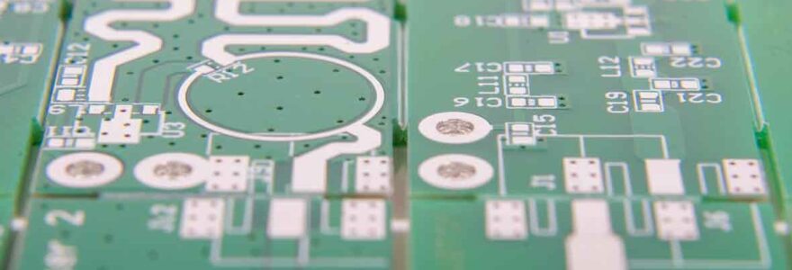
Panelization, a vital part of Printed Circuit Board (PCB) assembly, has emerged as a key player in enhancing efficiency and productivity. The process of panelization involves grouping multiple PCBs together onto a larger panel, thereby optimizing mass production. By using panels, the assembly line increases throughput, reduces handling time, and minimizes errors, leading to a more streamlined production process. icape-group.com provides comprehensive insights into this panelization process and its implementation in PCB assembly.
Choosing the correct panel support plays a crucial role in different types of PCB assembly. Material selection, size, and design are factors to consider for optimal support. The right support minimizes the risk of PCB damage during assembly, ensuring a high-quality end product. In addition, experts have identified techniques to detect and rectify common errors in using panelization, further enhancing the efficiency of PCB assembly.
Understanding the Roles of Tab Routing and V-Grooving in PCB Panelization
Embedded within the realm of PCB panelization, two pivotal processes emerge, namely tab routing and V-grooving. Both play significant roles in enhancing the efficiency of mass production.
Insights into Tab Routing in PCB Panelization
Tab routing, a widespread method in PCB panelization, involves creating small tabs that hold individual boards together on a larger panel. This technique enables simultaneous assembly of multiple boards, thereby improving production efficiency. However, it demands a careful design for manufacturability (DFM) review to ensure layout integrity. Avoidance of common errors, like placing components too close to the breakaway tabs, is essential for optimal results. Tab routing’s influence on the performance of a circuit board is substantial, often determining the ease of board separation and the overall quality of the final product.
Role of V-Grooving in Enhancing Panelization
Equally vital in PCB panelization is the V-grooving method. It involves creating a ‘V’ shaped groove on the top and bottom surfaces of the panel, facilitating easy breakaway. V-grooving, while offering a cleaner edge compared to tab routing, imposes design restrictions due to the reduced board area. This method suits projects that require a smooth edge finish and can handle the constraints on component placement near the edges. Technological advances continue to refine the V-grooving process for better precision and cost-effectiveness.
Choosing Between Tab Routing and V-Grooving
Deciding on the right panelization method is a critical step in PCB manufacturing. The choice between tab routing and V-grooving hinges on the project’s specific needs. For instance, tab routing is typically more suitable for complex boards with irregular shapes. On the other hand, V-grooving may be the preferred choice for simpler, rectangular boards requiring a neat edge finish. Adherence to relevant standards and regulations is pivotal to ensure the quality and safety of the panelized PCBs. To gain further insights, reliable resources, including research articles, online courses, or books on the subject, offer valuable guidance.
Panelization: A Cost-Effective Approach for Small and High-Quality PCB Production
In the realm of PCB production, panelization represents an approach that optimizes efficiency while minimizing costs. Panelization refers to the process of grouping several small board designs onto a larger board for simplified manufacturing. This technique offers substantial benefits, especially in the context of mass production. By consolidating multiple boards onto a single panel, manufacturers are able to streamline the assembly process, thereby reducing overall production costs.
Furthermore, panelization enhances the quality of the final product. The larger board size reduces the risk of damage during assembly and allows for more precise component placement. In an industry where precision is paramount, these advantages can lead to substantial improvements in the final product.
Panelization in PCB production serves as a viable solution for both small-scale and high-end manufacturers. Despite the initial costs associated with setting up the panelization process, the long-term savings in terms of reduced assembly time and improved product quality make it an economically sound choice. The challenge lies in effectively implementing panelization to reap its full benefits.
How PCB Material and Layer Choices Affect Panelization Efficiency
The impact of PCB material selection on panelization efficiency is often underestimated. Material type plays a crucial role in determining the success of panelization, a process fundamental to mass production. For instance, the use of copper, with its high thermal and electrical conductivity, significantly enhances panelization efficiency.
This data from illustrates the superiority of copper in terms of conductivity.
Comprehending the various layers of a PCB and their specific uses is equally critical. Each layer, be it a signal layer or a power plane, directly influences panelization efficiency. Therefore, strategic layer selection is paramount for optimizing mass production. To illustrate, a contrast between rigid and flex PCBs is enlightening. Rigid PCBs, often deployed in high-stress environments, offer enhanced durability. Flex PCBs, on the other hand, offer greater adaptability and can be tailored to fit the project’s specific requirements. Both have their unique advantages and the choice between them should be based on project specifications.